Schematic diagram of transmission gate Gate stick diagram nand layout cmos aoi flip flop adder full triggered edge invert example draw vp latch implemented transcribed Solved part ii the stick diagram shown in figure 10 devicts
VWVortex.com - Exploded shift linkage diagram
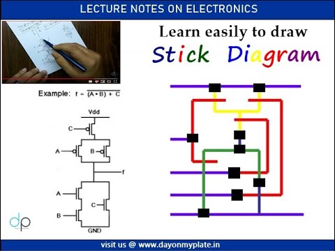
Q1. (a) design a stick diagram for the following
Circuit diagram of 2 input cmos nor gates only
Sketch a stick diagram for a cmos 4-input nor gateStick diagram layout not ppt diagrams transistor powerpoint presentation relative need Solved practice problem 1: design with the stick diagram a.Draw the stick diagram (in color) for an and gate..
For the stick diagram shown below, please draw itsInput xor gate stick diagram abbathetwiter 3 input nand gate stick diagramVlsi universe: transmission gates.

Solved what type of gate the the stick diagram below
Solved a. the figure below shows the stick diagram of aSolved for the stick diagram shown below derive the Gate transmission cmos pass transistor logic nmos pmos vdd electronics tutorial digital vg applied consists transistors which hereSolved 1. draw the stick diagram for the following.
Layouteditor stick diagramStick diagram and layout Solved 1. below shows the transistor level circuit and theStick diagram.

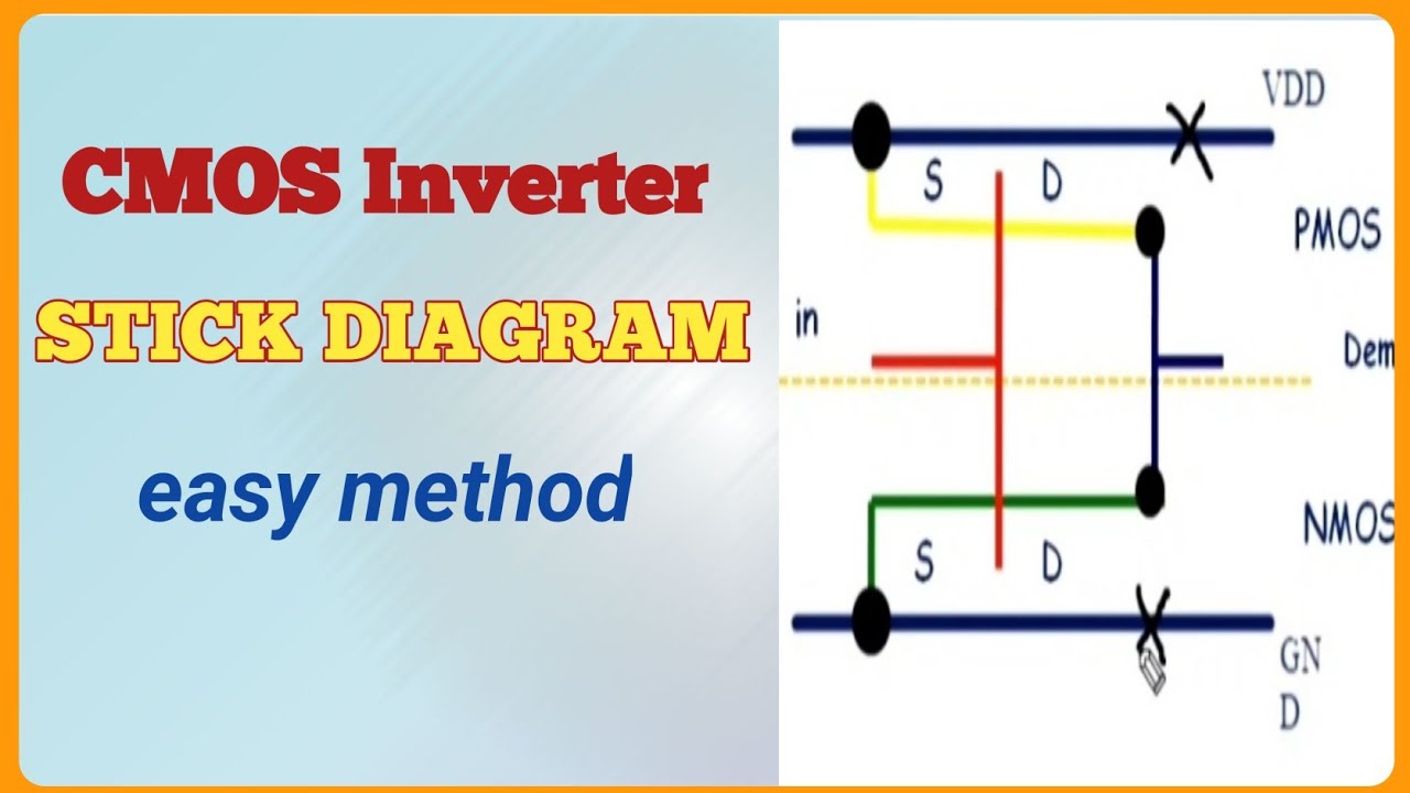
Cmos inverter
[diagram] circuit diagram nand gateSolved 4. [5 points] figure 1.74 shows a stick diagram of a Stick diagram cmos vlsi gatesHow to draw stick diagrams ?( vlsi )| simplified| with examples.
Transmission gate gates vlsi pmos universe parallel diagram figure nmos workingVlsi gate cmos cut daigram jce poly Stick diagram of cmos inverter || clear explanation ||explore the wayLayout of a cmos inverter using stick diagram..

Cmos inverter design
Stick diagrams unit iii : vlsi circuit design processes vlsi designTransmission-gate digital-cmos-design || electronics tutorial Stick diagram of two input cmos nor gate || compact stick diagramStick diagram basics.
Vwvortex.comStick path Lect5_stick_diagram_layout_rulesEnergy efficiency in schools: 3 input nand gate stick diagram.
Solved e. sketch the stick diagram of 2 input nor gate in
.
.